

media center

The 3D IC technology developed by XMC has emerged as a major player in the market for many years, and has secured a stable position in some hot areas such as processing in memory, 3D sensor ToF, etc. Recently, XMC registered the 3D IC technology as a new brand "3DLink", and presented the details in the ICCAD 2020 in Chongqing.
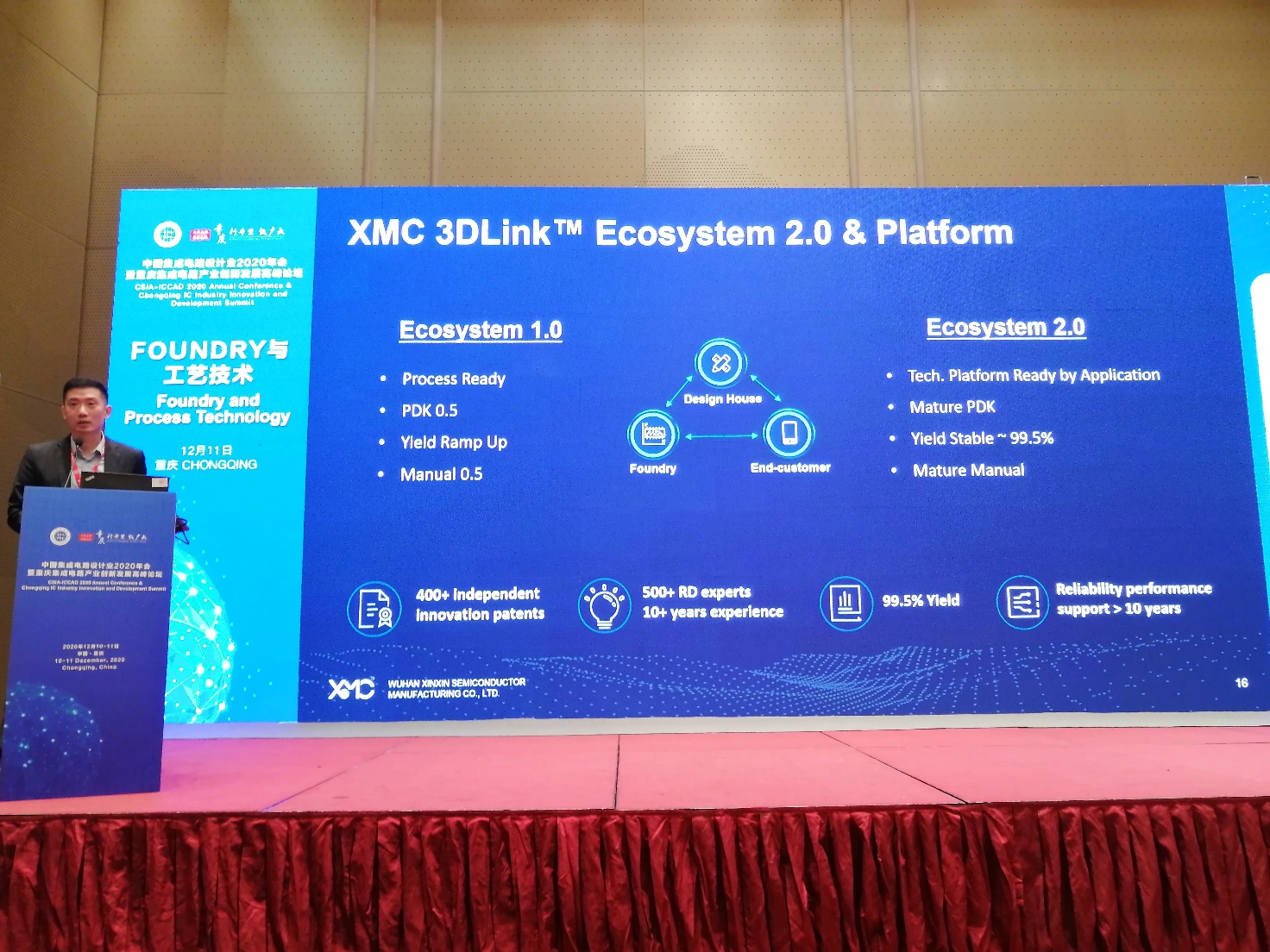
XMC has started planning 3D IC technology since 2012 with more than 8 years of experience in R&D and mass production, a bonding yield of 99.5%, and more than 400 innovation patents.
Today, the 3D IC technology has become a new focusing area for major global semiconductor companies, including TSMC and Samsung. TSMC announced early this year to roll out the new platform "3DFabric" by integrating the stacking to its packaging technology. As one of the leading manufacturers of 3D IC technology, XMC also made its new moves.
XMC announced that it will launch a new brand 3DLinkTM for 3D IC technology including two-wafer stacking technology which has started mass production, multiple-wafer stacking technology which has completed process R&D, chip-wafer heterogeneous integration technology which is still under development.
Shen Liang, Senior Director of XMC Foundry Business Division, indicated that in the past three years, ICCAD has become the stage for XMC to roll out its latest technologies, and the company released major R&D achievements of 3D IC technology at ICCAD annual conference every year.
At the ICCAD 2020 "Foundry and Process Technology" Subject Forum, Shen Liang delivered a presentation entitled "XMC 3DLinkTM - Solutions for Processing in Memory and High-Density Memory Chips", which inspired many innovative ideas in chip design.
According to the presentation, currently, there are several very popular application scenarios, which are very interesting in using the 3D IC technology, including processing in memory, 3D sensor technology TOF (Time-of-Flight), etc.
The 3D IC technology enables Cu-Cu direct interconnection between two wafers with different processes, thus to achieve higher interconnection density and alignment accuracy. High bandwidth and high-speed processing are achievable through direct interconnection. This technology provides innovative process and architecture for processing in memory chips. Making good use of the advantages of the 3D IC technology enables consumer electronic devices to be thinner and smaller with high performance.
For the same products, these advantages can't be achieved via the conventional semiconductor technology?
According to Shen Liang's analysis, processing in memory terminals have high requirements for bandwidth and processing. Nevertheless, it is achievable with advanced manufacturing technology, but the cost is high, and no guarantee can be made for the stability of continuous supply in the future. The wafer stacking technology of XMC can solve these problems while maintaining the advantages of high performance.
Two months ago, one of XMC’s customers released a processing in memory chip for edge processing. The chip combines 38nm customized Memory with 40nm SoC by using two-wafer stacking technology, and bursts out 1840GB interconnection bandwidth, realizing 25TOPS computation. Recently, Qualcomm released the latest Snapdragon 888 SoC, in which the computation of the processing in memory core with 5nm process is 26TOPS. In other words, we have successfully caught up with the performance of the products with the most advanced technology by combining mature process with advanced architecture. At present, the system based on this high-speed processing chip has been able to independently identify animals and plants offline through simple learning and training, and is learning human face recognition.
Another advantageous field of 3D IC technology is the "in-storage processing", which breaks the Von Neumann architecture, solves the problem of "storage wall" caused by the separation of processor and memory, and alleviates the latency and high power consumption caused by repeated memory access. According to his analysis, XMC’s two-wafer stacking technology allows direct stacking of Memory and Logic wafers, enabling rapid data transfer between different functional wafers with parallel efficient processing architecture.
As for wafer level HBM, Shen Liang pointed out that the multi-wafer stacking technology, which broke the micro-bump interconnection architecture of traditional package-level HBM, adopted the bumpless process to achieve direct bonding of multiple wafers and used the hybrid bonding process to achieve high-density interconnection.
Another area where 3D IC technology is well suited is the mainstream 3D sensor ToF.
3D sensor technology, specifically dToF (direct Time-of-Flight), has become the hottest topic around the world since Apple recently equipped the iPad and iPhone 12 with dToF lenses.
dToF is an active depth sensing technology, which directly calculates the distance from the measurement point by measuring the photon transmission time difference, and then starts the spatial modeling. It has the advantages of long detection distance, fast scanning speed and good resistance to light interference, and has been used in game consoles, AR/VR, intelligent vehicles and other fields.
In terms of this technology, a pulse laser is fired at the object under observation, and the photons reflected back from the object trigger the signal through ultra-sensitive single-photon avalanche diodes. As we know, the speed of light is 300,000 kilometers per second, so when measuring a person's face, the time difference between the photons reflected off the tip of the nose and the photons reflected off the philtrum is only 0.000003 seconds. Therefore, judging such a time difference in real time to calculate the distance requires a separate set of circuits for each trigger signal point for signal processing. In spatial modeling, a QVGA or VGA receiving point matrix is more needed. So even a small QVGA 320x240 matrix also requires higher connection bandwidth and processing speed to process these signals in real time. At this time, XMC 3DLinkTM stacking technology becomes the best solution.
According to Shen Liang, two-wafer stacking technology can meet the requirements of dToF products for data processing bandwidth and speed by stacking the photosensitive chips and logic circuits on top of each other. At the same time, it also meets the needs of low power consumption and small chips size of mobile phones.
From the above application scenarios, we can see several advantages of XMC’s 3D IC technology platform: innovative architecture, higher bandwidth, lower power consumption and latency, smaller chip size. So far, XMC’s 3DLinkTM has customized three specific process solutions for the pain points of high bandwidth, low latency and low power consumption required by storage, processing in memory chip and sensor respectively.
As for XMC’s 3DLinkTM technology platform, it has mature PDK, supporting customized development. Moreover, XMC hopes to cooperate with more customers in the industry, so that more high value-added solutions using 3DLinkTM technology can be implemented, and jointly create innovative IC products.
This article is reproduced from "Wenxin Voice".
No. 18 Gaoxin 4th Road, East Lake High-tech Development Zone,
Wuhan, Hubei, China
Tel: +86 27 87906000
Email: info@xmcwh.com